Intro to Computer Systems
Numbers In Different Bases
Before we talk about numbers in different bases, it's important to talk about what numbers are in base 10. Base 10 numbers are the numbers that we regularly use. It's called "base 10" because there are 10 unique symbols in the system (0 - 9). Each of those "symbols" represents a value. To get values higher than the value an individual symbol represents (max of 9) we use the position an combination of symbols.
Example:
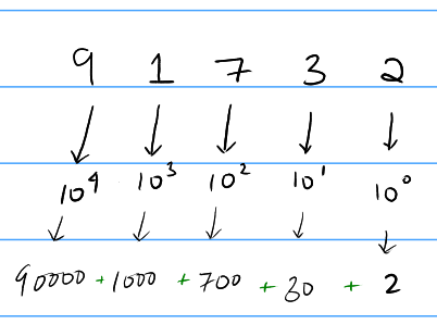
Here, we see that every time we move one digit to the left, the value of the digit increases by 10, this is not a coincidence; this is because of the fact that we use the base 10 system.
Binary Numbers
Binary Numbers are numbers in Base 2. This means that there are 2 symbols in the number system (0, 1). Similar to how every time we moved left the value increased 10 times, here the value increases 2 times (because it's base 2).
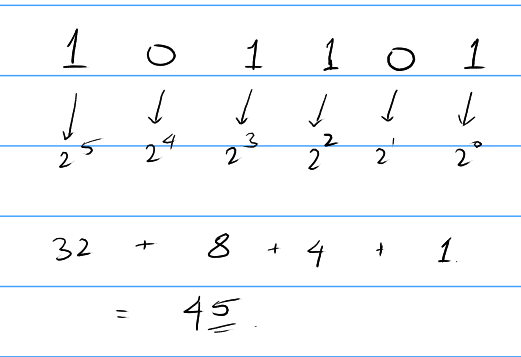
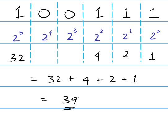
So, to convert a binary number to decimal, we just do the process to find the value in binary. Just to be clear, the numbers being talked about here are "unsigned" binary (which means only positive numbers).
Converting binary to decimal
- Write out the powers of 2 starting from 0 left to right.
- Add all the powers of 2 which correspond to the '1's in the original number.
Another example:
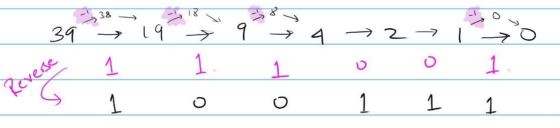
Converting decimal to binary
- Start by dividing the number by 2; if the number is odd, subtract by 1 and then divide by 2.
- Keep doing the above step until you reach 0.
- For every time you subtracted 1, you write down a 1 (pink ones in image.)
- Reverse the order of the 1s and 0s (mirror the number.)
You have the binary representation for the number!
Faster method
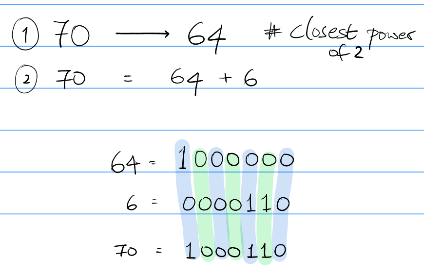
An alternate method to this would be to subtract or add the smallest possible number to a perfect power of 2 to find the representation of this number. This is my favorite method of finding the binary representation of a number. In my opinion, it's easy and has the lowest chance of calculation errors.
For some number $x \in \mathbb{Z}^{nonneg}$ we find the closest power of 2, say $t$.
If $t > x$:
then we rewrite $x$ as a difference of $t-1$ and $(t-1 \: -\: x)$. Then, we find the representation of $t-1$ (it's going to all 1's) and $(t-1 \:-\: x)$. Once we have the binary representations of the two numbers, we can just find their difference to find the original number.
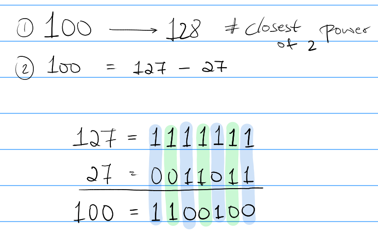
If $t > x$:
then we rewrite $x$ as $t + (x - t)$. Then, we find the representation of $t$ (it's going to be one 1 and all 0's) and $(x - t)$. Once we have the binary representations of the two numbers, we can just find their sum to find the original number.
NOTE: If the second number is a number for which the binary representation is hard, you can always use the method again for that number. In fact, with just knowing that 0 is "0" and 1 is "1" in binary and knowing the powers of 2, you can find all other number just by performing the above operation repeatedly.
Hexadecimal Numbers
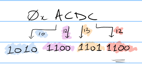
Hexadecimal numbers are numbers in base 16. We use 16 symbols to represent numbers in the following order of increasing value: 0, 1, 2, 3, 4, 5, 6, 7, 8, 9, A, B, C, D, E, F. A - F hold the values from 10 to 15.
Since both hexadecimal numbers and binary numbers are both in bases are are powers of 2, i.e. binary has a base of 21 and hex has a base of 24 this allows really easy conversion between the 2 bases.
Converting from Binary to Hexadecimal
- Split the binary number into chunks of 4 starting from the right.
- If the left most chunk doesn't have 4, you can just add '0's (similar to how 05 = 5 in decimal).
- Find the value of each "chunk" and write the corresponding symbol in hex.
We prefix the hexadecimal numbers with 0x to indicate that they have been written in hexadecimal. This is to avoid confusion with decimal or any other base.

NOTE: You can only pad zeros to the left if the number is either positive or is unsigned. In our case, the numbers are unsigned binary numbers.
Converting from Hexadecimal to Binary
- Each symbol has a value from 0 to 15 and we just write the binary representation to each of the symbols and you have the binary number.
Signed Binary
So far, we've only established positive number and we need to think about some way to represent negative numbers. In decimal, we just prefix a "-" to our number and it denotes the number as negative. However, in computers we only have access to 2 symbols, so these are some options we have.
- Option 1: Add a bit to denote the sign (0 -> +ve, 1 -> -ve).
- Option 2: 1s compliment, we're not going to discuss this here.
- Option 3: 2s compliment, this is the best choice.
Option 1 problems: IF you add -1 and +1 you don't get 0 which is an obvious problem.
Option 3 advantage: If you add -1 and +1 you get 0 by design.
Option 3 disadvantage: You have to have a "fixed length" and that cannot change during an operation.
Signed Decimal to Signed Binary
If value is positive:
This follows the same process as unsigned binary numbers, expect one rule: All positive numbers must start with a 0. So after the conversion of a positive number, make sure to prefix the number with a 0.
Example:
8 -> 1000 -> 01000 (8 in signed binary)
15 -> 1111 -> 01111 (15 in signed binary)
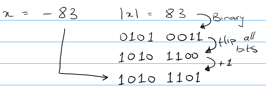
If value is negative:
- Find the positive version of the number (with the first 0)
- Flip all the bits (0s becomes 1s and 1s becomes 0s).
- Add 1 to the number.
- This gives us the signed binary representation for the number.
IMPORTANT:
- All positive numbers in binary start with a 0.
- Any number of leading 0s before a positive number doesn't change it's value.
- All negative numbers in binary start with a 1.
- Any number of leading 1s before a negative number doesn't change it's value.
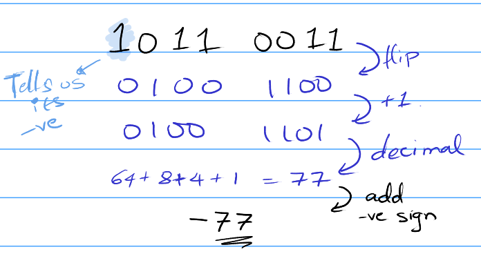
Signed Binary to Signed Decimal
If it's positive, you can just do the same process as unsigned binary to find the value of the number in decimal. ( Tell if a number is positive by looking at it's first bit, if it's 0 then it's positive else negative. )
If it's negative:
- Find the positive version of the binary number using the following steps
- Flip all the bits and add 1.
- Convert this positive binary number to decimal.
- Add a "negative" sign to the decimal number.
Unsigned Binary Floating Point
If we have a floating point number in decimal, such as 29.640625 would be represented as 011101.101001. The non-decimal part of the number is converted the same way as regular binary, for the fractional part of the number, we keep subtracting negative powers of 2 from the value till it reaches 0.
Example:
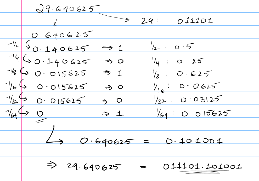
And to find the decimal value of a binary floating point value, we just do this in the reverse order. We sum all the respective negative powers of 2.
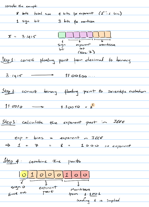
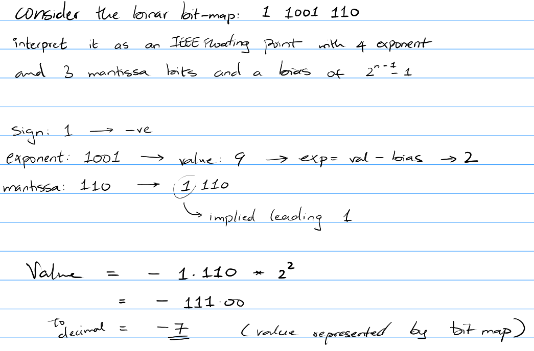
IEEE Floating Point
IEEE is a standard that has been established as a form of storing floating point values in a computer.
The way IEEE works, given a number of bits, we create 3 categories:
- The sign bit
- The exponent
- The mantissa
Here's a website that does IEEE conversion: Floating point converter
Since we want to store both positive and negative values for the exponent, rather than using 2's compliment (which causes some issues in math operations for this particular purpose), they just shift the 0. Ex: 0 - 12 actually represents -12 - -1, 13 represents a 0 and 14-24 represents 1-12.
It's easiest to explain this with an example.
Floating point to IEEE representation
From IEEE representation to floating point
Commonly used "defaults"
- IEEE floating point is commonly used for 32-bit or 64-bit values (
float and double data type in Java or C).
- The bias is almost always going to be
2^(n-1) - 1.
- The number of exponent bits in 32-bit floats is USUALLY 8 bits.
- The number of exponent bits in 64-bit floats is USUALLY 11 bits.
- The values that IEEE fails to represent are non-continuous chunks in the rational number line.
Denormalized Exponent
Let's consider the following 8-bit floating point (as in the example) number: 0 0000 000. This should evaluate an exponent of -7 and a mantissa of 1.000 (since the 1) is implied. Okay, what about 0 0111 000, the exponent would be 0 and the mantissa would be 1 again.
Do you see an issue here? There's no way to store 0! Since the 1 in the mantissa is implied, there's no way for us to represent 0.
So, to solve this problem, we say that if the exponent has all zeroes (value would be -bias), then a 0 is implied in the mantissa, rather than a 1.
When ALL the exponent bits are 0 then we consider the value of the exponent to be -bias + 1 (rather than -bias) and the leading bit assumed in the mantissa becomes a 0.
Example of denormalized number:

Zero is stored as just all zeros:

Notes:
- Some sources state that if all the exponent bits are zero, then the number is taken to be 0, but I couldn't find this anywhere else and I'm going to choose to ignore this.
- Thanks to discord user:
@Meluke#6971 for pointing out a mistake in my denormalized IEEE.
Special Value
-
When all the exponent bits are 1 AND the mantissa is all 0s, then the value of the floating point is inf (infinity).
-
When all the exponent bits are 1 AND the mantissa is NOT all 0s,
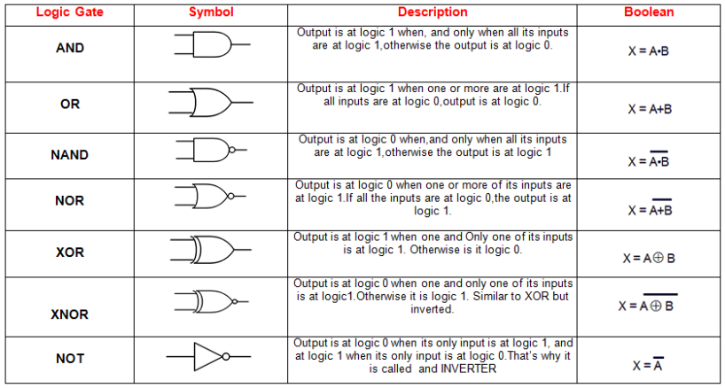
Boolean Logic
Symbols Syntax
X.Y → Logical AND
X+Y → Logical OR
X'  → Logical NOT
X⊕Y → Logical XOR
Note, NOT also sometimes is represented as X with a bar on top.
- NOT(A): True if A is False; False if A is True.
- AND(A, B): True if both A and B are true.
- OR(A, B): True if either A is true or B is true.
- XOR(A, B): True if A if True or B is True but not if both are True.
Demorgans Laws
(X + Y)' → X' . Y'
(X . Y)' → X' + Y'
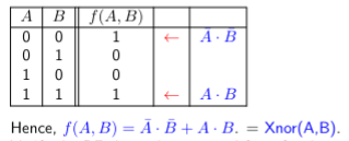
Construct Boolean Function from Truth Table
Algorithm:
i/p -> Input
o/p -> Output
- Identify each row that has a '1' in the right-most (o/p) column.
- For each such row, AND the i/p variables. Use the variable if it is a '1'; else use the negation of the variable.
- OR the results from each '1' row, to obtain the final expression.
Example:
Logic Circuits
Relay Switches
A relay is a form of an electric switch. A relay can be a binary digit: 1 if the Relay is closed and 0 is the relay is open. It is a switch that is controlled by an electric current.
They consist of a coil of wire around a conducting core. A current running through the coil magnetizes the conducting core which attracts a flexible metal strip that makes contact with the OUT terminal to complete the circuit.
We represent logical gates in circuits in the following way:
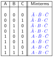
Canonical Form
A boolean function can be expressed in many ways. There are canonical forms. Canonical forms contain "sums" of the "product" terms or vice versa. A product term, in which the literal or its complement appears exactly once is called a minterm.
Example of minterms:
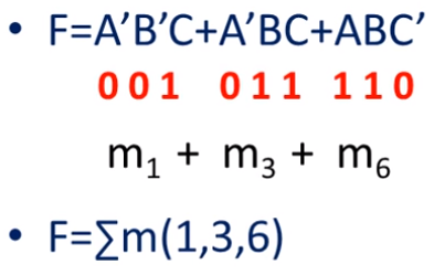
Another example of min terms to represent a function:
Maxterms are the compliment of maxterm where we take the sum of the variables and for a 0 we just use the variable and for 1 we use the compliment.
Example:
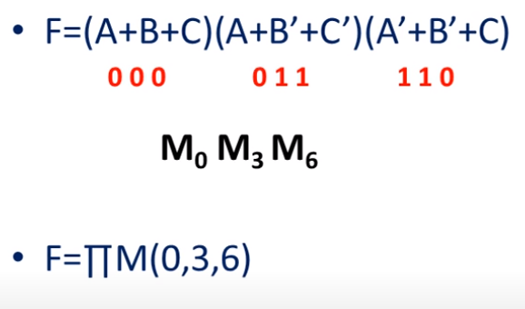
You can see that we write a function as either the sum of minterms or the product of maxterms.
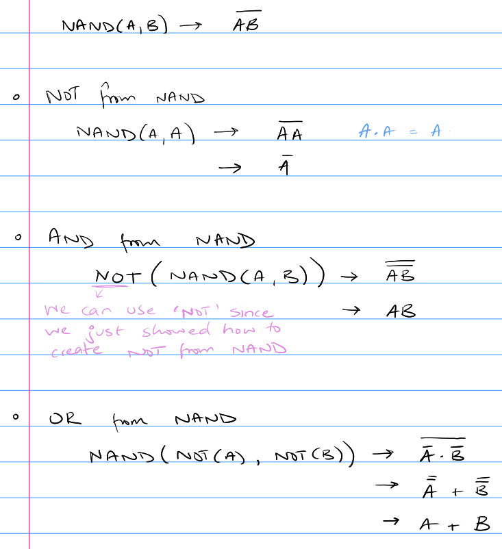
NAND As Universal Gate
Using de morgan's laws and some basic boolean algebra laws, we can show that the NAND gate is a universal gate.
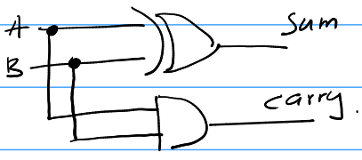
Half-Adder
A half-adder is just a system that adds 2 binary numbers together. The sum of 2 binary numbers can be seen as the output of an XOR gate. The carry of the 2 numbers can be seen as AND of inputs. So, we can create a half-adder using an XOR and an AND gate.
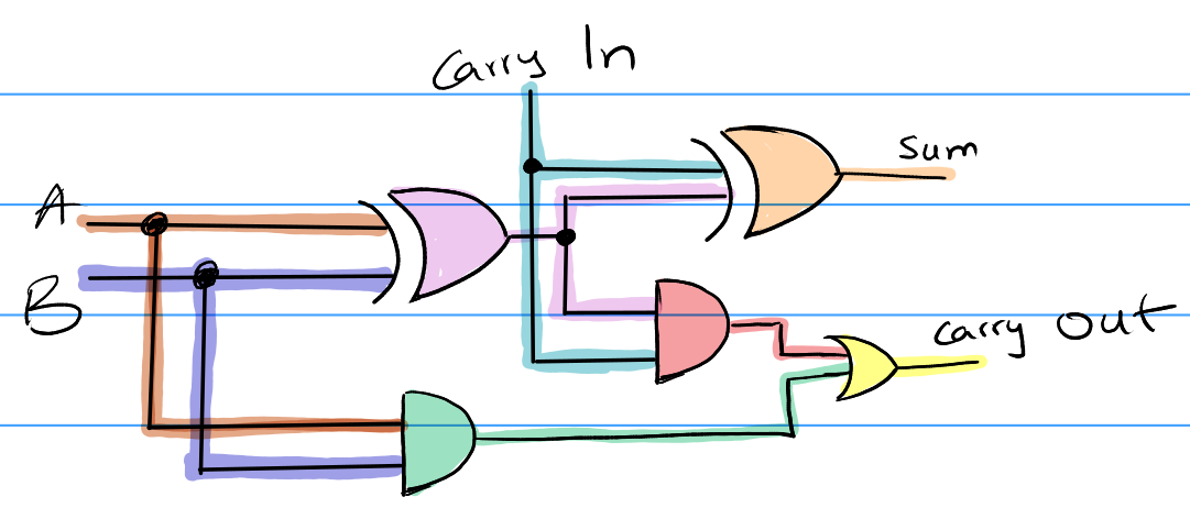
Full-Adder
A full-adder is a system that can add 3 numbers: A, B and Carry-in. That can be designed in the following way
Combinatorial Circuits
- A combinatorial circuit consists of gates representing boolean connectives, that is free of feedback loops.
- A combinatorial circuit has no state. Its output depends on the instantaneous inputs.
- The output doesn't matter on previous state / time, just the current inputs matter.
Multiplexer (Mux)
- A Mux has 2n inputs. Only the selected input is allowed to be routed to the output.
- A Mux is a switch that routes one of the inputs to the output.
- The number of selectors is equal to
log<sub>2</sub>(no_of_inputs).
An example for a mux would be a 2 to 1 mux. It has 2 inputs and 1 selector.
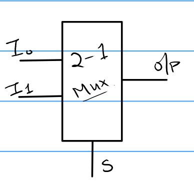
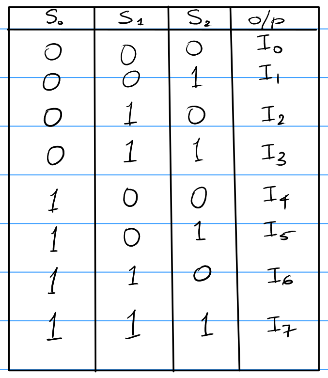
The input selected is based on the number described by the selector bits.

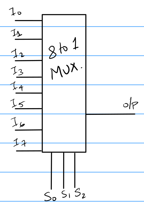
8 to 1 mux. It has 8 inputs and 3 selector bits.
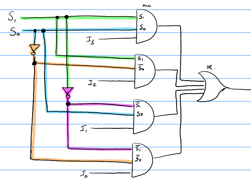
Here is an example of how a mux may be designed on the inside. This is a 4-1 mux, with 2 selector bits.
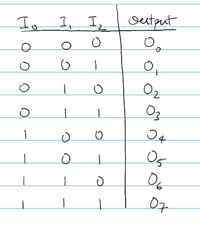
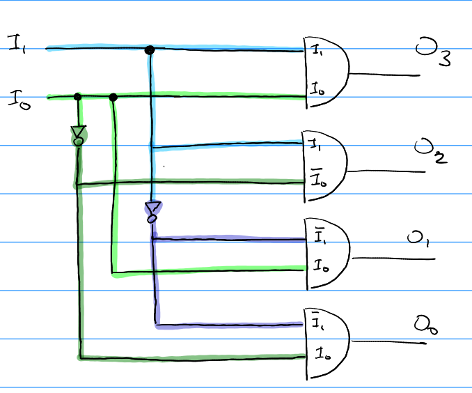
Decoder
A decoder basically does the opposite of what a Mux does, in the sense that it takes in a few inputs and turns on exactly one output line based on a particular state of inputs.
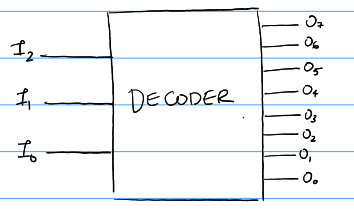
Truth Table
The internal circuitry of a decoder
Sequential Logic
- Here the output depends on the current state of the system and the input given to it.
- Time plays a role.
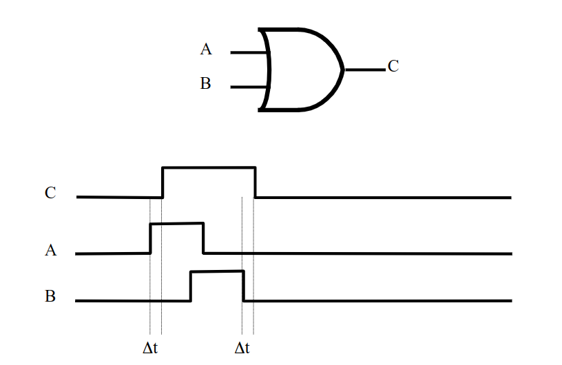
Gate Timing
In the real world, gates take some time to react to a particular input and logic is based on electric voltages which take time to change. We denote "gate delay" (time taken for gate to respond to input) with Δt
Feedback Loop
This is when you connect the output of a particular gate to its own input.
Here's the diagram of a nor gate connected to itself:
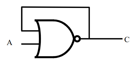
If A was 0, the output would be 1 but if the output is 1 then the input that's connected to the output would be 1 and that would cause the output to change to 0 and so on and so fourth.
It's possible to use feedback in a circuit that is predictable and stable. It is harder to tell what is going on, but it's possible to figure out the output at some initial time, use that output to determine the next output and so on.
S-R Latch
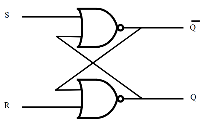
An S-R latch is a particularly useful feedback circuit that used to store memory in computers. The S stands for "Set" (as in "Set output to 1") and R stand for "Reset" (as in "Reset output to 0").
In this configuration, if we power S then the value of Q is going to stay 1 until we power R. And if we power R then Q is going to stay 0 until we power S. You can see how this can be used to "store" a bit.
We can create a truth table for the outputs of the S-R latch, but since the output depends on the time, we can have a truth table for some initial state and some next state.
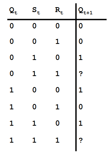
The ? in the truth table exists due to the unpredictable nature of the state. Since the gates produced aren't perfect, the final state of the system depends on the way the defects in the gates affect the slight timing of the gates.
Clocked S-R Latch
Inside a computer we want the output of gates to change only at specific times. All operations in a computer are synchronized. We can add some circuitry to make sure that the changes only occur at the clock "edges" (when the clock changes from 0 to 1).
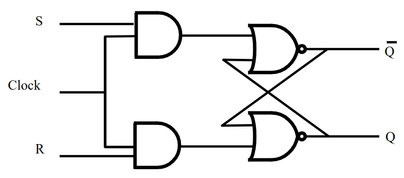
Q only changes when the clock is a 1.- If clock is
0, neither S or R reach the NOR gates.
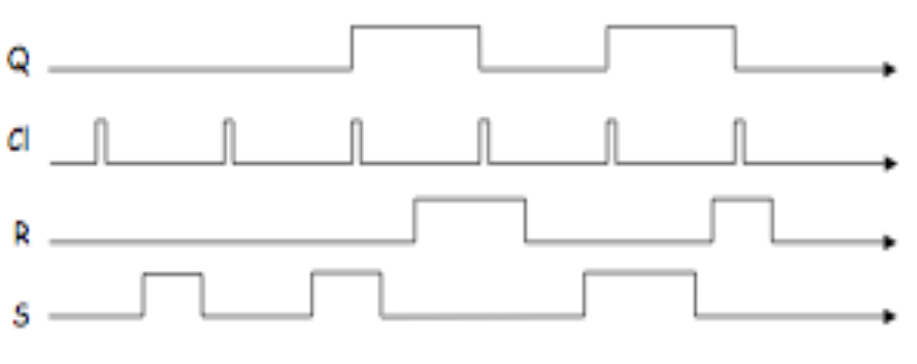
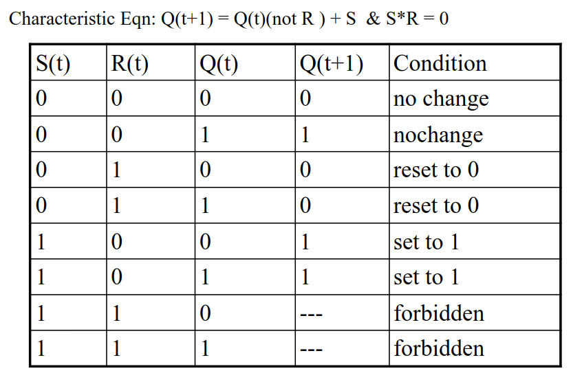
The characteristic table and equation for the clocked S-R Latch.
The D Latch
In the S-R Latch, since if both S and R are 1, we have unpredictable behaviour, we can solve this problem by forcing them to be different. A D-latch is clocked by definition.
The design for a D latch:
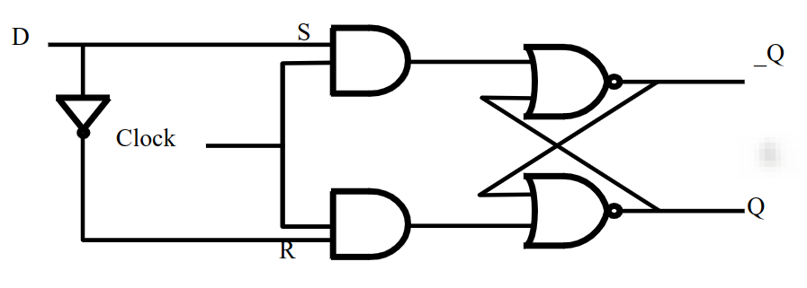
Now we have just one input, D. If D is powered, when the clock changes from 1 to 0, the circuit will remember the value 1 (Q=1). If D is powered off, when the clock changes from 1 to 0, the circuit will remember the value 0 (Q=0).
D Flip-Flops
The difference between a flip flop and a latch is that the flip-flop is "edge-triggered" type of memory circuit while the latch is "level-triggered" type.
(TODO: I'm going to explain this further in some other notes to which I'll add a link here)
A simple explanation of the D Flip-Flop: It have one input (and one clock input), when the clock is on the rising edge, the output of the flip-flop matches the input. It DELAYS the input passed into the flip-flop up to one clock tick. These form the bases for some forms of volatile memory (RAM).
Memory
Memory Hierarchy
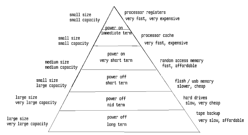
The faster memory, like for the processor register and the L1 cache are made of flip-flops. Main memory, commonly referred to as RAM, is made of different technology.
8 Bit Memory
We can use 8 D Flip-Flops to create an 8 bit memory unit. We have 8 inputs that we want to store, all are written at the same time.
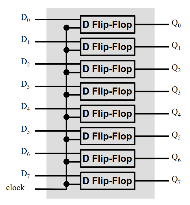
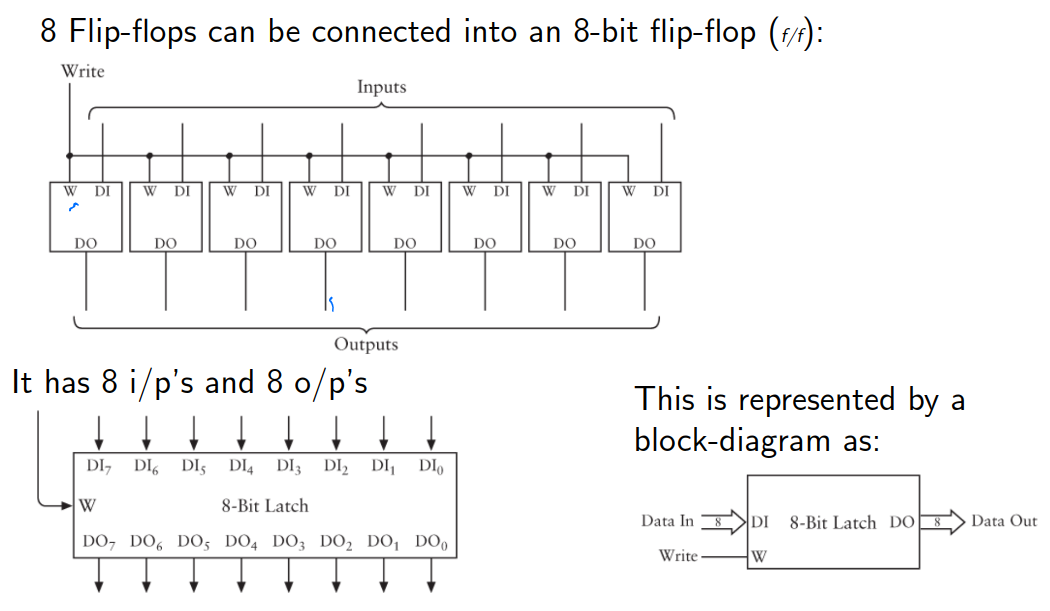
The 8 bit memory can be accessed using an address and can be set as a chunk. We can read the memory similar using the address in an 8-bit chunk. Usually, there's a "write-enable" bit that will have to be powered on to allow data to be written to memory.
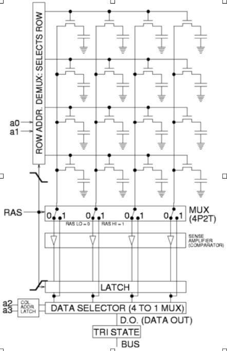
Dynamic RAM (DRAM): The capacitance of each "Field Effect Transistor" allows the storage of a charge. The transistor itself acts as a switch that allows the "memory" to be read. Over time, the charge drains away from the capacitor and hence needs to be continuously refreshed ( several hundred times/sec ) even if the power is on. Hence it has the name "dynamic".
Expanding the word size
In our 8-bit memory, we could read and write to 8-bit chunks of memory using an address. How can we change this so that the number of bits written to and read from at a given address is higher? We can just stack 8-bit chunks at the same address to expand the word size.
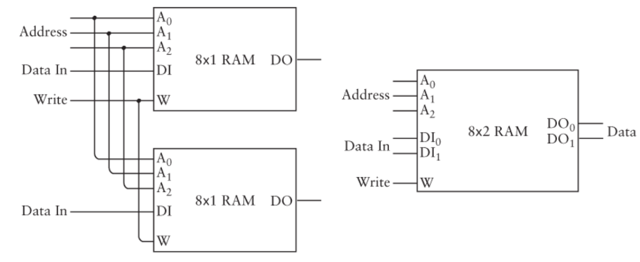
The above configuration allows us to store 16-bits at a given address rather than 8. This makes it 8 x 2 RAM
Expanding memory
If we want to increase the memory and the addresses at the same time we add a selector bit and select between the different ram modules.
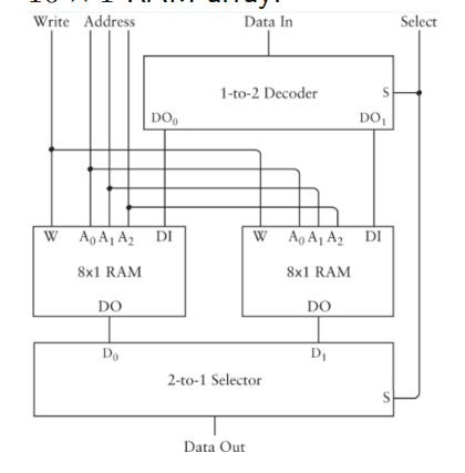
The "selector" bit acts as a 4th address bit making it 16 x 1 RAM
The addressability of a machine is the size of the most basic unit that can be named by an address.
-
A Byte-addressable machine is one where you can reference memory in 8-bit units (no smaller). This is the most common form of memory addressability.
-
A Word-addressable machine is one where you can reference memory in word sizes. Typically this would be the size of an integer (data type). This is common among RISC computers.
The width of the MAR (and hence the width of the Address Bus) determines the number of memory locations that can be addressed. The width of the Data Bus determines the number of bits that can be transferred in/out of memory at a time.
Memory Sizes
Memory Capacity is the number of bytes it can hold. Memory size is represented in the form L x W where L is the number of locations and W is the size of each word in bits.
Hence 64K x 8 RAM can hold:
2^6 * 2^10 x 8 => 2^16 bytes.
Writing and Reading from memory
During the process of writing and reading from memory, the MAR (Memory address register) holds the address (from the CPU) of the data in memory. The MBR (Memory buffer register) or MDR (Memory data register) hold the bits that are to be written to the location specified in MAR or the memory that is read from that location.
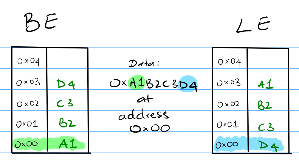
Multi-byte Memory Layout (L/B Endian)
Multi-byte memory such as 8K x 32 must pick an order for the bytes within each word. This depends on the manufacturer of the CPU.
-
Big Endian (BE): The most significant byte is stored at the lowest address. Example, for 8K x 32, which has 4 bytes, consider the memory contents: 0xA1B2C3D4 (32 bits), stored at the address a. The bytes will be stored A1 at a, B2 at a+1, C3 at a+2, and D4 at a+3. IBM Computer, ARM, and SPARC are examples of architectures that use BE.
-
Little Endian (LE): The least significant byte is stored at the lowest address. Example, for 8K x 32, which has 4 bytes, consider the memory contents: 0xA1B2C3D4, stored at a. The bytes will be stored D4 at a, C3 at a + 1, B2 at a + 2, and A1 at a + 3. Intel, all x-86 and x86-64, AMD, M1/M2 macs are examples of architectures that use LE.
Additional Notes
RAM stands for Random Access Memory. It's a type of memory where any (accessible) location of memory, on average, takes the same amount of time to access.
Smaller, faster, and more expensive memory known as Static Random Access Memory (SRAM) is used for the registers and caches. SRAM is made of flip-flops (requiring one flip-flop per bit). Each flip-flop needs about 6 transistors to construct. This makes then very expensive.
Main memory, since the mid-70s made of DRAM (Dynamic RAM), where each bit is stored as a charge on a leaky capacitor (actually a '1' bit is the presence of charge on the capacitance on a single transistor). Dynamic memory needs to be “refreshed” every 64 milliseconds. The refresh cycle compensates for the charge that "leaks" away. This is one of the things that makes DRAM memory slow. DRAM modules however can be manufactured very cheaply (requiring one transistor per bit). Memory is now manufactured with the same technology as other chips - reducing the cost/byte of storage dramatically since the 90’s. A further advantage of DRAMs is that they use much less power than SRAMs.
Computer Organization
Registers
-
A register is a group of n flip-flops (usually), each storing a bit. This is typically read as a unit.
-
Registers are short term storage with very fast access for the processor (CPU).
-
Most computers move data into registers before performing operations on the data.
-
Some registers have specific hardware function while others are general purpose registers (GPR).
Special Registers
Along with the general purpose registers, the CPU has several special purpose registers, not directly accessible to the programmer (sometimes), that are vital to the proper functioning of the computer.
-
PC (Program Counter): Holds the memory address of the next instruction to be fetched and executed. In 32-bit x86 systems, this is the EIP (IP - Instruction pointer, cause Intel wanted to be annoying).
-
IR (Instruction Register): Holds the current instruction fetched from memory while being decoded and the operands for the instruction are fetched.
-
MAR (Memory Address Register): This register holds a memory address and is used to access that location in memory.
-
MDR or MBR (Memory Data Register or Memory Buffer Register): Holds the value accessed from or to be written to the memory location specified in the MAR.
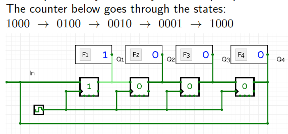
Counters
Digital counters are vital for the operation of a computer. Counters go through a pre-determined sequence of states. The number of bits in a counter is the number of flip-flops used.
There are UP and DOWN counters, mod k counters, ring counters etc.
The simplest is the Ring Counter: A ring counter is a circular shift register which is initiated such that only one of its flip-flops is the state one while others are in their zero states.
Counters also act as frequency dividers, a frequency divider is something that changes the timing of the clock used.
Instruction Set Architecture (ISA)
Every CPU that is designed has an associated Instruction Set that comes along with it (ISA). These are the operations that the CPU can perform and the bits that represent those operations.
Here's an example, this is the ISA for the LC-3 (Little Computer 3)
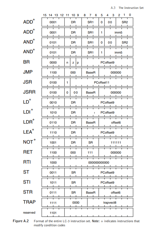
As you can see, it specifics where in the instruction the operands have to be placed and what each of bits represent.
Instructions are loaded into the CPU using the IR (instruction register) and the CPU goes through different phases to decode and execute the instruction.
I'm not going to elaborate on the details of how this works since I already have those details under these notes. I've explained the instruction cycle in great details over there.
Processor Architecture
Accumulator Machine
An accumulator machine has a single register, whose contents can be combined with a single operand from memory. These types of machines are called 1-address machines.
Such machines require instructions to load and store the accumulator.
Stack Machines
A stack machine (JVM, the HP-15C, etc) have no operands. The utilize the stack to read operands and they write the results to the top of the stack. Stack machines are referred to as 0-address machines.
The operands are always on the system stack. Instructions are executed by popping operands off the stack, performing the operation and storing the result back on the stack.
General Register Machines
These are typically load/store machines (RISC, MIPS). They have small amounts of very fast memory, in the form of a register file. Machines typically have specialized instructions to load/store values to/from memory. These can be 2 or 3-address machines.
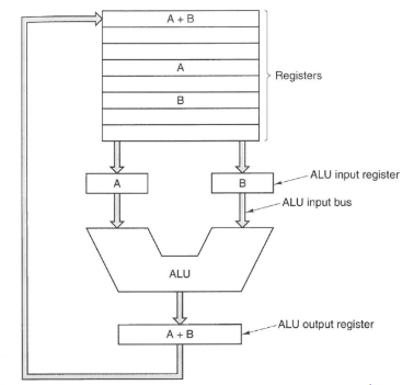
Parts of the CPU
-
ALU: The Arithmetic and Logic Unit performs all the actual arithmetic and logic operations like Add, And, etc. It (typically) receives the operands from the registers, carries out the computation specified and stored the results back to the registers. It completes its operations within a clock cycle (not always true).
-
Register file: A set of general purpose registers that store temporary working data. Registers are very fast, temporary memory. A computer needs at least one general purpose register.
-
PC: The Program Counter contains the address of the next instruction to be executed. In normal operation, it is automatically incremented by one unit. It can also be loaded with an arbitrary address for a branch or jump instruction.
-
PSR: The Program Status Register has flags (one bit signals) that are set depending upon the last instruction. Flags for things like if the result was negative, zero, positive, if there was an overflow, etc. This is used to carry out branch instructions.
-
CU: The Control Unit controls the CPU. The unit generates the signals that cause data to be loaded into registers, it signals the ALU to carry out the correct operations, etc. The CU interprets the instruction in the IR. The CU uses a stream of clock pulses and the op-code to generate all the signals that control the buses, memory and registers.
Datapath
The ALU and the registers, along with their internal buses form the datapath. The datapath is an important part of the processor design. To a considerable extent, the datapath defines what the machine can do. The process of bringing the two operands to the ALU, carrying out the operating and storing the result is called the datapath cycle. The faster the datapath cycle, the faster the computer.
System Bus
All (sequential) computer system have the same basic organization. This organization has three units: the CPU, the memory sub-system and the I/O sub-system, inter-connected by the system bus. Physically, a bus is a collection of parallel wires. Typically, the system bus consists of separate set of writes for transmitting.
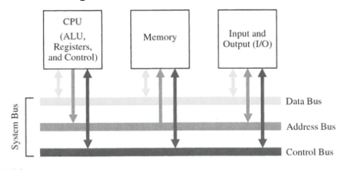
Typically the width of the data bus is the same as the word size of the computer. The lines of the data bus transmit those many bits at a time.
The control bus delivers control signals from the CPU to the Memory or I/O device. The control bus is different from the other two since it's a collection of uni-directional control signals (say indicating "read" or "write" to memory). There are very few control signals that pass from the I/O devices to the CPU or the Memory to the CPU.
x86 Intel Assembly
This section is going to refer to the ATT format for intel assembly (the alternate is intel format). So, all the registers are designated with % and immediate constants have a $ prefix.
I found this website to be the most helpful resource when trying to learn assembly. However, I'll be talking about the basics of it in here as well.
We will also be talking about 32-bit assembly and not x86-64 assembly. A lot of what is done in 32-bit is the same in 64-bit but there are some differences and the register names are different as well.
Introduction
For each instruction in assembly, you pass a couple things to the processor. The op-code, which specifies the operation to be performed and 1 to 2 operands.
An instruction in assembly takes the form:
<opcode> <operands1>, <operand2>
Here's an example of Intel x86 assembly:
push   %ebp
mov    %esp,%ebp
sub    $0x10,%esp
call   0x1208 <__x86.get_pc_thunk.ax>
add    $0x2e6c,%eax
mov    0x8(%ebp),%eax
mov    (%eax),%eax
mov    %eax,-0x4(%ebp)
Operands
We can pass one of the following as operands to an instruction:
- A literal:
$1234 or 0xFF12 (raw values)
- A cpu register:
%ebp or $eax (registers)
- A memory evaluation:
8(%ebp, 2) (this is calculated to be an address)
Addressing Modes
- Indirect:
(%eax) <- use memory location specified by %eax.
- Displacement:
8(%ebp) <- at memory location %ebp + 8.
- Indexed:
d(Rb, Ri, s) <- calculated as (Rb + d) + (Ri * s)
- Rb -> Base register (register)
- Ri -> Index register (register)
- s -> Scale factor (number)
- d -> Displacement (number)
Note: For indexed mode, all the elements are optional but are positional.
Instructions
mov_ source, destination
The move instruction copies the data from the source to the destination. At most, one of the operands can be a memory evaluation. movl %(eax), %(ebp) is not a valid instruction.
The _ is replaced by a size. Example: movl moves a long.
Examples:
movl %ebp, %eax  # copies contents of ebp into eax
movl (%ebp), %eax # copies contents at location ebp into eax
movl %eax, %(ebp) # copies eax into memory location specified by ebp
lea_ source, destination
The lea instruction stands for "load effective address". This instruction is used to evaluate a memory address expression and store the result of the evaluation of the expressing in the destination register.
Examples:
leal 0x8(%ebp, %eax, 4) %eax
The above instruction calculates the memory expression ((%ebp + 8) + (%eax * 4)) and stores the result of that operation in eax.
The C Compiler sometimes uses lea instructions to perform arithmetic operation if it thinks it's more convenient.
sub_ a, b
The sub instruction finds the difference between a and b (b - a) are stores the result in b.
Examples:
subl %ebp %eax # Calculates %eax - %ebp and stores result in %eax
subl %(ebp) %eax # Calculates %eax - value at address %ebp are stores in %eax
add_ a, b
The add instruction is similar to the sub instruction, it calculates the sum of a and b and stores the result in b.
Examples:
addl %eax %ebp # Calculates %ebp + %eax and stores in %ebp
imul_ a, b
Similar to add but performs the product operation rather than addition, stores the result in b.
sal_ val, reg/mem
This performs a left shift on the reg/mem location by the value specified by val. It stores the results back into the reg/mem.
push_ mem/reg
Push the value stored in the operand onto the stack. The push operation automatically increments the stack pointer.
pop_ mem/reg
Pop the top value stored in the stack into the location specified. The pop operation automatically decrements the stack pointer.
jmp
The jmp instruction causes the program to jump to the location specified by the label. This is used to create loops in programs. This works by updating the PC (program counter) to the address of the label. This jump is unconditional.
Example:
jmp .L2 # Jump to location L2
j
The instruction is used to jump if a condition is is satisfied. This internally uses the PSR register which stores the condition codes from the last operation.
Most j<condition> jump are performed immediately after the cmp instruction. The cmp instruction performs a subtraction and only updates the flags and does not store the result.
Example:
cmp a, b
je L2 # jump if a = b

cmp a, b
jne L2 # jump if a != b

cmp a, b
jg L2 # jump if b > a (not that the operands are revered)
There are other operations that can be performed, the Intel x86 ISA is HUGE.
Here's a couple of useful sources: